Dear Professor Rob Marano,
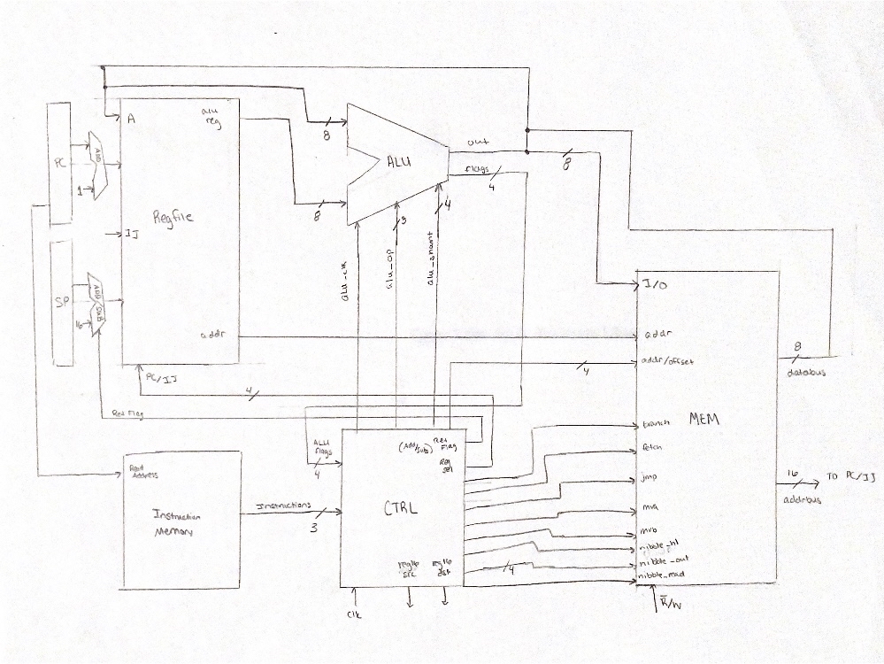
Before writing any Verilog, we first needed to describe a somewhat rigorous Instruction Set Architecture (ISA). Ideally, such an abstract model would exist before writing anything in a Hardware Description Language (HDL) since it serves as the basis for how software controls a Central Processing Unit (CPU). Given that this was our first time designing a CPU from the ground up, much of the ISA was in constant flux as we slowly converged on our final design.
Inspiration for JAVK came from the GameBoy's LR35902 and the MOS Technology 6502. We most heavily borrowed on the idea of an accumulator as this allowed us to squeeze all our instructions into a single byte, avoiding the need for variable-length instructions.
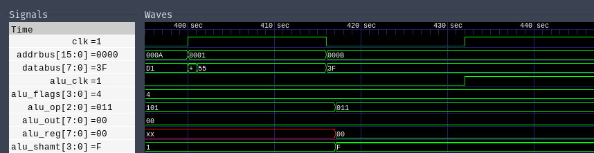
JAVK has an 8-bit Arithmetic Logic Unit (ALU) that supports the following operations:
- adding
- subtracting
- negation
- bitwise and
- bitwise inclusive or
- bitwise exclusive or
- logical shifts left
- logical shifts right
The ALU also has the following output flags:
- negative (N)
- zero (Z)
- carry (C)
- overflow (V)
On a rising clock edge, the ALU performs the configured operation and updates the output and flags accordingly.
JAVK consists of 20 addressable registers. Of these, 16 are 8-bit, while the remaining four are 16-bit. Of these 16-bit registers, two map directly on top of two 8-bit registers allowing for manipulation using an 8-bit ALU.
Register Map:

+-------+-------+
|   A   |   B   |
+-------+-------+
|   C   |   D   |
+-------+-------+
|   E   |   F   |
+-------+-------+
|   G   |   H   |
+-------+-------+
|   I   =   J   |
+-------+-------+
|   K   =   L   |
+-------+-------+
|   M   |   N   |
+-------+-------+
|   O   |   Z   |
+-------+-------+
|      P C      |
+-------+-------+
|      S P      |
+-------+-------+
| Register | Index | Size |
|---|---|---|
A |
0b0000 |
8b |
B |
0b0001 |
8b |
C |
0b0010 |
8b |
D |
0b0011 |
8b |
E |
0b0100 |
8b |
F |
0b0101 |
8b |
G |
0b0110 |
8b |
H |
0b0111 |
8b |
I |
0b1000 |
8b |
J |
0b1001 |
8b |
K |
0b1010 |
8b |
L |
0b1011 |
8b |
M |
0b1100 |
8b |
N |
0b1101 |
8b |
O |
0b1110 |
8b |
Z |
0b1111 |
8b |
PC |
0b00 |
16b |
SP |
0b01 |
16b |
IJ |
0b10 |
16b |
KL |
0b11 |
16b |
A- accumulator. The result of all arithmetic operations reside in this register. This register is also used as the first operand for all ALU operations (with exception of negation). This register is also the only register which can load and store data of the databus.F- flags. All modifiable and readable CPU flags reside in this register.I- high byte of theIJregister.J- low byte of theIJregister.K- high byte of theKLregister.L- low byte of theKLregister.Z- zero. The zero register is always contains a constant value of zero. All writes to this register are discarded.PC- program counter. The program counter holds the address of the next instruction to be executed.SP- stack pointer. The stack pointer stores the address of the last program request in a stack.IJ- intended jump. The intended jump register serves two primary roles: containing the address from where data is read to/written from theAregister or the address which execution should jump to.KL- keep link. Upon a jump with link (JPL), thePCregister will be incremented and stored in this register.
| Instruction | Format | Encoding | Description |
|---|---|---|---|
ADD |
R |
0b0000 XXXX |
Add |
SUD |
R |
0b0001 XXXX |
Subtract |
NEG |
R |
0b0010 XXXX |
Negate |
AND |
R |
0b0011 XXXX |
AND |
ORR |
R |
0b0100 XXXX |
Inclusive OR |
EOR |
R |
0b0101 XXXX |
Exclusive OR |
LSL |
I |
0b0110 XXXX |
Logical shift left |
LSR |
I |
0b0111 XXXX |
Logical shift right |
MVA |
R |
0b1000 XXXX |
Move A register |
MVB |
R |
0b1001 XXXX |
Move 16-bit register |
LNL |
I |
0b1010 XXXX |
Load nibble low |
LNH |
I |
0b1011 XXXX |
Load nibble high |
LDB |
D |
0b1100 XXXX |
Load byte |
STB |
D |
0b1101 XXXX |
Store byte |
JMP |
B |
0b1110 XXXX |
Jump |
JPL |
B |
0b1111 XXXX |
Jump (with link) |
As the table above would suggest, all instructions in JAVK consist of a single byte where the high nibble corresponds to the opcode, and the lower nibble corresponds to the operand.
Arithmetic operations take up eight of the total 16 instructions
available in JAVK and take up the 0b0XXX address range. By mapping
the arithmetic operations to this address range, the lower three bits
can be directly passed to the ALU's opcode input and enabled when the
MSB of the opcode is a zero.
For most operations, the operand corresponds to the register index of the second operand to the ALU. The exceptions to this convention are the two logical shift operations, as they use the four bits to specify a shift amount for the value in the accumulator.
The two movement operations take up the 0b100X address range.
MVA (move A) is the first of the two movement operations and moves
the contents of the A register to the specified operand register. The
only exception is the Z register which maintains the constant value of
zero.
MVB (move "big") is the second of the two movement operations and
moves the contents of one 16-bit register to another. Since there are
only four 16-bit registers, this allows for specifying both a source and
a destination register. The high two bits of the operand correspond
with the destination register, and the low two bits correspond with the
source register.
The two immediate loading operations take up the 0b101X address range.
Both operations store the nibble as the operand. The only distinction
between the two operations is which nibble they replace in the A
register.
The two data operations take up the 0b0110X address range.
Both operations store an address offset in the operand. The operations
always add the unsigned offset to the address in the IJ register.
Both set the address bus to the newly computed address, with the only
distinction between the two is that one reads the databus into the A
register while the other writes the contents of the A register to the
databus.
The two branch operations take up the 0b0111X address range.
Both operations store the branch condition in the operand. Both
instructions branch to the address stored in the IJ register. The
main distinction between the two instructions is that JPL is a jump
with a link. On a branch, it stores the return address in the KL and
the SP into the IJ register. If the programmer sets the return
flag, SP gets incremented by 16 instead of being decremented by 16.
Condition codes:
| Encoding | Alias | Description | Flags |
|---|---|---|---|
0b0000 |
EQ |
Equal | Z |
0b0001 |
NE |
Not equal | !Z |
0b0010 |
HS |
Unsigned greater than or equal | C |
0b0011 |
LO |
Unsigned less than | !C |
0b0100 |
MI |
Negative | N |
0b0101 |
PL |
Positive or zero | !N |
0b0110 |
VS |
Overflow set | V |
0b0111 |
VC |
Overflow clear | !V |
0b1000 |
HI |
Unsigned greater | C && !Z |
0b1001 |
LS |
Unsigned less than or equal | !(C && !Z) |
0b1010 |
GE |
Greater than or equal | N == V |
0b1011 |
LT |
Less than | N != V |
0b1100 |
GT |
Greater than | !Z && (N == V) |
0b1101 |
LE |
Less than or equal | !(!Z && (N == V) |
0b1110 |
AL |
Always | Any |
0b1111 |
NV |
Always | Any |
When branching into a subroutine, the A, B, C, D, E, G, and
H registers serve as argument registers. If more than seven registers
are needed, the address to a region in memory where additional arguments
reside should be moved into the G and H registers; the G register
should contain the high byte, and the H register should contain the
low byte.
The return value should be placed in the A register. If a 16-bit
value is to be returned, the high byte should be placed in the A
register, while the low byte should be placed in the B register. If
the return value is larger than 16-bits, the caller should follow the
same convention as done with G and H if there are too many
arguments, but place the segment of memory where the return value should
reside before any additional arguments.
When entering a subroutine, the KL register contains the return
address and IJ contains the address of SP, this allows for the
programmer to backup any registers as they seem fit. While in a
subroutine, the M, N, and O registers must be saved before use.
To return from a subroutine, the programmer must set the return flag in
the flags register and place the return address into the IJ register.
R-type format:
I-type format:
D-type format:
B-type format:
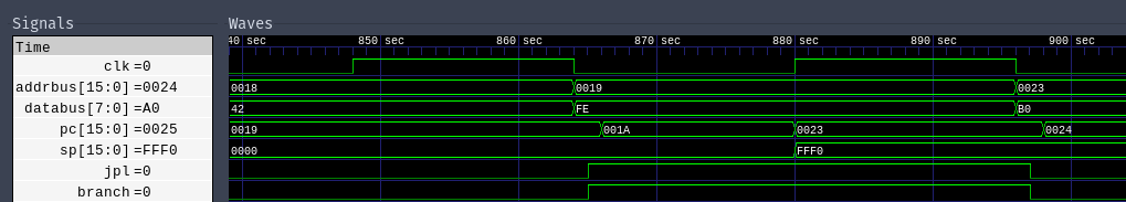
All instructions take one clock cycle to execute. On the falling edge, an instruction is fetched into the processor and decoded internally. The controller then decodes the instruction and primes all internal components for the rising clock edge. Once the rising clock edge is detected, the instruction is executed, and the result is written to the appropriate location.
Copyright (C) 2022 Jacob Koziej <[email protected]>
Copyright (C) 2022 Ani Vardanyan <[email protected]>
Licensed under the CC BY-NC-SA 4.0.