A from-scratch, hand-soldered flight controller built to close the gap between writing embedded firmware and actually understanding the hardware it runs on.

-1f6feb?style=flat-square)


CoreSen-V2, fully populated. LQFP-100 STM32F407VGT6, salvaged MPU-9250, hand-soldered in one four-hour session.
- Why This Board Exists
- At a Glance
- The Build Timelapse
- System Architecture
- Hardware Deep Dive
- Peripheral and Pin Map
- PCB Layout
- Engineering Tradeoffs
- Known Issues and V3 Roadmap
- Bring-Up Procedure
- Repository Structure
- Building the Firmware
- Manufacturing It Yourself
- What I Learned
- License
I spend most of my time on the firmware side — bare-metal register work, peripheral drivers, control loops. That is a comfortable place to sit, but it is also a place where the hardware becomes a black box. You read a datasheet, you write to a register, something happens, and you never really ask why the board was built that way.
CoreSen-V2 was my way out of that. I wanted to design a board where I could point at every single component and explain what it does, why it is there, and what breaks if I remove it. Not a dev-board with a sensor bolted on — the whole thing, from the power tree up.
It took roughly two months of design across schematic capture, footprint work, and layout, and about four hours of hand-soldering to populate. The result is a compact flight controller built around the STM32F407VGT6 with a high-rate SPI IMU, four motor outputs, three UARTs, and the analogue sensing lines a real flight stack expects.
This repository is the complete design: schematics, layout, Gerbers, BOM, firmware project, and the reference material I used to get there.
| Microcontroller | STM32F407VGT6 — ARM Cortex-M4F, 168 MHz, 1 MB Flash, 192 KB SRAM, LQFP-100 |
| IMU | MPU-9250, 9-DoF, on SPI1 (salvaged from a dead Navio2) |
| Clock source | 8 MHz crystal (Y1) with 10 pF load capacitors |
| Motor outputs | 4× timer-driven PWM (PA0–PA3) |
| Serial | 3× UART broken out (UART1, UART3, UART6) |
| RC input | PPM on PC9 |
| Analogue sensing | Battery voltage, current, RSSI (PC1 / PC3 / PC2) |
| Aux bus | I²C pads with on-board pull-ups (PB6 / PB7) |
| Power input | DC barrel/battery header, or USB 5 V, Schottky OR-ed |
| Regulation | AMS1117-5.0 → AMS1117-3.3 cascade |
| Debug | SWD (SWDIO / SWDCLK / NRST) on a 5-pin header |
| Board | 2-layer, 264 pads, 130 vias, 112 nets, 0 unrouted |
| EDA tool | KiCad 9.0.6 |
| Design time | ~2 months |
| Assembly | Hand-soldered, ~4 hours, hot air + drag soldering |
Drag-soldering a 100-pin LQFP with 0.5 mm pitch, then placing every passive by hand, is mostly an exercise in patience and flux management. The full four-hour session is condensed below.
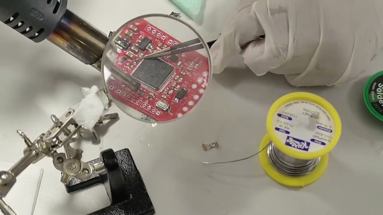
Click to watch the full assembly on YouTube.
Replace
YOUR_VIDEO_IDin both URLs above with your YouTube video ID (the part afterwatch?v=).
flowchart TB
    subgraph PWR["Power"]
        VDC["VDC input<br/>battery"] --> U4["U4<br/>AMS1117-5.0"]
        USB5["USB 5 V<br/>via J5"] --> D5["D5 · BAT54C<br/>Schottky OR"]
        U4 --> D5
        D5 --> U3["U3<br/>AMS1117-3.3"]
        U3 --> R33["+3.3 V rail"]
        R33 --> FB["FB1 · 120R<br/>ferrite bead"]
        FB --> VDDA["+3.3 VA<br/>analogue rail"]
    end

    subgraph CORE["Compute"]
        MCU["U1 · STM32F407VGT6<br/>Cortex-M4F @ 168 MHz"]
        Y1["Y1 · 8 MHz XTAL"] --> MCU
        SW1["SW1 · Reset"] --> MCU
    end

    R33 --> MCU
    VDDA --> MCU

    subgraph SENSE["Sensing"]
        IMU["U2 · MPU-9250<br/>accel + gyro + mag"]
    end

    subgraph IO["I/O"]
        MOT["4× PWM<br/>motor outputs"]
        UARTS["UART1 / UART3 / UART6"]
        PPM["PPM receiver in"]
        ADC["VBAT / Current / RSSI"]
        I2C["I²C aux pads"]
        BUZZ["Buzzer"]
        LEDS["D1 / D2 status LEDs"]
    end

    MCU <-->|"SPI1 + INT"| IMU
    MCU --> MOT
    MCU <--> UARTS
    PPM --> MCU
    ADC --> MCU
    MCU <--> I2C
    MCU --> BUZZ
    MCU --> LEDS

    subgraph DBG["Debug + Comms"]
        SWD["SWD header"]
        USBIF["USB 2.0 FS<br/>J5 micro-B"]
    end

    SWD <--> MCU
    USBIF <--> MCU

Complete schematic — MCU block, IMU block, and regulator block.
The STM32F407VGT6 was chosen for headroom rather than minimalism. A Cortex-M4F at 168 MHz with a hardware FPU means attitude estimation — quaternion maths, complementary or EKF filtering — runs in single-precision float without the usual embedded contortions of fixed-point arithmetic. The 100-pin package also gave me enough exposed I/O to break out everything a flight stack might want, instead of multiplexing peripherals against each other.
The core clock comes from Y1, an 8 MHz crystal, loaded with two 10 pF capacitors (C15, C16), feeding the internal PLL. 8 MHz was deliberate: it divides cleanly to the 168 MHz core clock and the 48 MHz clock the USB OTG FS peripheral requires, so USB and full-speed core operation can coexist without a second oscillator.
Reset and boot: SW1 pulls NRST low through a 100 nF filter cap (C12), and R1 (10 kΩ) holds BOOT0 down so the chip always boots from Flash unless deliberately overridden.
Power comes in from one of two sources and converges on a single 3.3 V rail:
VDC (battery) ──► U4 AMS1117-5.0 ──┐
                                   ├──► D5 (BAT54C dual Schottky) ──► U3 AMS1117-3.3 ──► +3.3 V ──► FB1 (120R) ──► +3.3 VA
USB 5 V (J5)  ─────────────────────┘
The BAT54C is the interesting part. It is a dual Schottky in a single package, wired as an OR-ing diode so the board can be powered from USB on the bench or from the flight battery in the air, without back-feeding the USB host and without needing a jumper. Whichever rail is higher wins.
FB1 (120 Ω ferrite bead) splits a dedicated +3.3VA analogue rail off the main digital rail, feeding VDDA and VREF+. Without this, every switching edge from 168 MHz digital activity couples straight into the ADC reference, and battery-voltage and current readings pick up noise proportional to how busy the CPU is. The bead plus C9 (10 nF) and C10 (1 µF) forms a low-pass filter that keeps the analogue domain quiet.
D3 is a power-good LED on the 3.3 V rail with a series current-limiting resistor — the cheapest possible "is this board alive" indicator, and worth every millimetre of board space during bring-up.
PWR_FLAG symbols are placed on VDC, +5 V, and USB_5V so KiCad's ERC understands where power actually originates rather than warning about undriven power nets.
This was the single biggest sourcing constraint of the project.
A flight controller lives or dies on how fast it can read its gyroscope. Attitude loops want gyro samples at 1–8 kHz; anything slower and you are integrating stale data into your attitude estimate, which shows up as sluggish or oscillatory control. I²C at 400 kHz simply cannot sustain that for a 9-DoF sensor once you account for register addressing overhead. SPI was non-negotiable.
The problem: almost every IMU breakout available to me locally in Türkiye was an I²C-only module. Bare SPI-capable IMU ICs, in single quantities, with reasonable shipping time, were not realistically obtainable.
The solution was salvage. I had a dead Navio2 board with an intact MPU-9250 on it. I hot-air rework removed the sensor, cleaned the pads, and gave it a second life on CoreSen-V2. Desoldering a QFN without cooking it is nerve-wracking, but the MPU-9250 is genuinely excellent for its footprint — 3-axis gyro, 3-axis accelerometer, and an AK8963 magnetometer in a 3×3 mm QFN-24 — and it natively supports SPI up to 20 MHz for sensor registers.
How it is wired:
| MPU-9250 pin | Function in SPI mode | STM32 pin |
|---|---|---|
SCL/SCLK |
SPI clock | PA5 (SPI1_SCK) |
SDA/MOSI |
Master out, slave in | PA7 (SPI1_MOSI) |
AD0/MISO |
Master in, slave out | PA6 (SPI1_MISO) |
nCS |
Chip select, active low | PA4 (GPIO) |
INT |
Data-ready interrupt | PC4 (EXTI) |
Note the pin-name trap: in I²C mode those pins are SCL, SDA, and AD0, which is why the schematic net labels still read GYRO_SCL / GYRO_SDA / GYRO_SDO. The MPU-9250 switches to SPI automatically when nCS is pulled low, and the same silicon pins take on completely different roles. Reading the pin table without reading §7 of the datasheet is a very easy way to route this backwards.
REGOUT gets its own 1 µF (C23) for the internal LDO, and the supply is decoupled with a 100 nF / 10 nF / 100 nF / 1 µF network (C17–C20) split across VDD and VDDIO.
Why the interrupt line matters: polling the IMU wastes bus bandwidth and introduces jitter between sample time and read time. Wiring INT to an EXTI pin means the control loop is driven by the sensor's own sample clock, which is exactly what you want for a deterministic attitude loop.
J5 is a micro-B connector feeding the STM32's integrated USB 2.0 Full Speed transceiver directly on PA11 (D−) and PA12 (D+). The F4 series has the transceiver on-die, so no external PHY and no 22 Ω series resistors are needed — the impedance matching is internal.
Layout for USB followed ST's AN4879 (included in datasheets/): D+ and D− routed as a tightly coupled differential pair, matched length, kept short, with no vias or stubs along the pair.
A resistor divider off the USB 5 V rail provides VBUS sensing so firmware can tell whether it is bench-connected or flying.
Debug is plain SWD — SWDIO on PA13, SWDCLK on PA14, plus NRST and 3.3 V/GND on a 5-pin header. Any ST-LINK V2 clone will program it.
The STM32F407 has six VDD pins plus VBAT and VDDA, and ST's guidance is one 100 nF close to each supply pin plus bulk. The board follows this:
| Capacitor(s) | Value | Purpose |
|---|---|---|
| C1–C7 | 100 nF | One per VDD pin, placed as close to the package as layout allowed |
| C8 | 10 µF | Bulk reservoir for the digital rail |
| C9, C10 | 10 nF, 1 µF | VDDA filtering behind FB1 |
| C11 | 1 µF | VREF+ decoupling |
| C12 | 100 nF | NRST filter — stops spurious resets from noise on the reset line |
| C13, C14 | see note | VCAP_1 / VCAP_2, internal core regulator stabilisation |
| C15, C16 | 10 pF | Crystal load capacitors |
| C21, C22 | 22 µF | AMS1117-5.0 input/output |
| C24, C25 | 22 µF | AMS1117-3.3 input/output |
VCAP note: these are currently populated at 100 nF. See Known Issues — the F407 datasheet calls for 2.2 µF low-ESR here, and this is a genuine deviation I caught while documenting the board.
| Function | Net name | STM32 pin | Package pin | Peripheral |
|---|---|---|---|---|
| Motor 1 | MOTOR1 |
PA0 | 23 | TIM2_CH1 / TIM5_CH1 |
| Motor 2 | MOTOR2 |
PA1 | 24 | TIM2_CH2 / TIM5_CH2 |
| Motor 3 | MOTOR3 |
PA2 | 25 | TIM2_CH3 / TIM5_CH3 |
| Motor 4 | MOTOR4 |
PA3 | 26 | TIM2_CH4 / TIM5_CH4 |
| IMU chip select | GYRO_CS |
PA4 | 29 | GPIO output |
| IMU clock | GYRO_SCL |
PA5 | 30 | SPI1_SCK |
| IMU MISO | GYRO_SDO |
PA6 | 31 | SPI1_MISO |
| IMU MOSI | GYRO_SDA |
PA7 | 32 | SPI1_MOSI |
| IMU interrupt | GYRO_INT |
PC4 | 33 | EXTI4 |
| Buzzer | BUZZER |
PA8 | 67 | GPIO / TIM1_CH1 |
| Telemetry TX | UART1_TX |
PA9 | 68 | USART1_TX |
| Telemetry RX | UART1_RX |
PA10 | 69 | USART1_RX |
| USB data − | USB_DM |
PA11 | 70 | OTG_FS_DM |
| USB data + | USB_DP |
PA12 | 71 | OTG_FS_DP |
| Debug data | SWDIO |
PA13 | 72 | SWD |
| Debug clock | SWDCLK |
PA14 | 76 | SWD |
| GPS / aux TX | UART3_TX |
PB10 | 47 | USART3_TX |
| GPS / aux RX | UART3_RX |
PB11 | 48 | USART3_RX |
| Status LED 1 | LED1 |
PB3 | 89 | GPIO (D2) |
| Status LED 2 | LED2 |
PB4 | 90 | GPIO (D1) |
| I²C clock pad | SCL_PAD |
PB6 | 92 | I2C1_SCL |
| I²C data pad | SDA_PAD |
PB7 | 93 | I2C1_SDA |
| Battery voltage | VBAT_PAD |
PC1 | 16 | ADC1_IN11 |
| RSSI input | RSSI_PAD |
PC2 | 17 | ADC1_IN12 |
| Current sense | CURRENT_PAD |
PC3 | 18 | ADC1_IN13 |
| RX / ESC TX | UART6_TX |
PC6 | 63 | USART6_TX |
| RX / ESC RX | UART6_RX |
PC7 | 64 | USART6_RX |
| RC input | PPM_IN |
PC9 | 66 | TIM3_CH4 input capture |
| Reset | MCU_RST |
NRST | 14 | SW1 + header |
| Boot select | BOOT0 |
BOOT0 | 94 | 10 kΩ pulldown |
Motors 1–4 sit on PA0–PA3 deliberately: all four map to channels of the same 32-bit timer (TIM2 or TIM5), so all four PWM outputs share one timebase and update in the same cycle. Spreading them across different timers would introduce phase skew between motors — small, but not something you want in a control loop.
Test points are placed on the motor outputs, IMU SPI lines, buzzer, and all three analogue sense pads, which made scope probing during bring-up substantially less painful than probing package pins.

Layout in the KiCad PCB editor — routing, silkscreen, and courtyards visible.
| Metric | Value |
|---|---|
| Copper layers | 2 (F.Cu / B.Cu) |
| Pads | 264 |
| Vias | 130 |
| Track segments | 565 |
| Nets | 112 |
| Unrouted | 0 |
| Mounting holes | 4 |
Routing was ordered by how much each net cared about being routed badly:
- Crystal loop first. Y1 and its load caps are placed tight against the OSC_IN/OSC_OUT pins with the shortest possible loop area, and no other signals routed underneath. An oscillator that will not start is one of the more miserable bring-up failures to debug.
- Decoupling second. Each 100 nF sits on the same side as its VDD pin with a via to ground directly at the pad, so the current loop from cap to pin to plane stays small. Decoupling routed as a long trace is decorative, not functional.
- USB differential pair third. Matched, tightly coupled, short, no stubs.
- IMU SPI fourth. Kept short and grouped so all four lines see similar propagation delay, and routed away from the switching current paths of the regulators.
- Everything else. Motor outputs, UARTs, and analogue pads fanned out to board-edge headers.
IMU placement was chosen to sit away from the regulators — the AMS1117 devices are the only meaningful heat sources on the board, and thermal gradients across a MEMS gyro produce bias drift. It is also kept off the mounting-hole stress paths, since board flex mechanically couples into the sensor package and shows up as low-frequency noise in the accelerometer.
Form factor was a compromise with my own hands. I could have shrunk this board considerably by tightening component spacing, but every millimetre I removed made hand-soldering harder. Since this board was always going to be assembled by me with a soldering iron rather than by a pick-and-place machine, the design rule became: if I cannot get a fine-tip iron and tweezers in there, it is too tight.
The most useful thing this project taught me had nothing to do with routing or register maps. It was that hardware design is a negotiation between three things that are almost never simultaneously satisfiable: what you want, what you can afford, and what you can actually get hold of.
| I wanted | Constraint | What I did | What it cost me |
|---|---|---|---|
| SPI IMU at 8 kHz | Only I²C modules available locally | Salvaged an MPU-9250 from a dead Navio2 via hot-air rework | Hours of rework risk; non-reproducible BOM |
| 4-layer board with solid ground plane | 2-layer is dramatically cheaper in single quantities | Built 2-layer with careful return-path management | Compromised return paths; noisier analogue domain |
| Switching regulator for the 5 V rail | Linear regs were what I had, and simpler to route | AMS1117-5.0 linear | Significant heat dissipation from a high-voltage input |
| Machine assembly | No access, and cost | Hand-soldered LQFP-100 + 0603/0402 passives | Four hours and a lot of flux |
| Compact footprint | Must remain hand-solderable | Relaxed component spacing | Board is larger than it strictly needs to be |
Several components I would have reached for first simply were not obtainable in Türkiye in single quantities without a multi-week lead time. Working around that pushed me into solutions I would never have found if the parts had just been sitting on a shelf — the Navio2 salvage in particular. Constraint turned out to be a better teacher than budget would have been.
I would rather document the problems honestly than pretend the board is perfect. These are the issues I have identified, in rough order of severity.
| # | Issue | Impact | Planned fix |
|---|---|---|---|
| 1 | VCAP_1/VCAP_2 populated at 100 nF. The STM32F407 datasheet specifies 2.2 µF low-ESR capacitors on these pins for internal core-regulator stability. | Potential core regulator instability, especially at 168 MHz under load. May manifest as intermittent resets or erratic behaviour rather than a clean failure. | Swap to 2.2 µF X5R/X7R with ESR < 2 Ω. Same footprint, drop-in on the existing board. |
| 2 | 2-layer stack-up. No solid ground plane means return currents take whatever path the pour allows. | Degraded EMI performance, worse ADC noise floor, higher risk of USB signal integrity issues. | Move to 4-layer: signal / GND / power / signal. Cost delta is small at prototype quantities now. |
| 3 | Linear regulation from battery voltage. A 3S LiPo at 12.6 V through an AMS1117-5.0 at 200 mA dissipates over 1.5 W in a SOT-223. | Thermal problem; also wasteful of flight battery capacity. | Replace U4 with a synchronous buck (e.g. TPS5430 or MP2315 class). |
| 4 | No USB ESD protection. D+/D− go straight to the MCU. AN4879 recommends a TVS array. | A single static discharge on the connector can kill the USB peripheral or the MCU. | Add a USBLC6-2SC6 across the pair at the connector. |
| 5 | No reverse-polarity protection on the DC input. | Wiring the battery backwards destroys the board. | Add a P-channel MOSFET ideal-diode on VDC. |
| 6 | Single IMU, no redundancy. | Any sensor failure is a total loss of attitude estimation. | Add a barometer (BMP280/DPS310) and, ideally, a second IMU on a separate SPI bus. |
| 7 | No SD card or flight logging. | Cannot post-analyse a flight. | SDIO is available on the F407 — add a microSD socket. |
| 8 | Salvaged IMU makes the BOM non-reproducible. | Nobody else can build this exactly. | Move to a currently-manufactured SPI IMU (ICM-42688-P or BMI270) for V3. |
| Component | Status |
|---|---|
| CubeMX project + clock tree config | ✅ Done |
| SWD connectivity, blink | ✅ Done |
| SPI1 driver, MPU-9250 WHO_AM_I readback | 🚧 In progress |
| Gyro/accel register configuration + DMA reads | 🚧 In progress |
| AK8963 magnetometer via auxiliary bus | 📋 Planned |
| Sensor fusion (complementary → EKF) | 📋 Planned |
| PWM output driver (OneShot125 / DShot) | 📋 Planned |
| PPM input capture | 📋 Planned |
| ADC battery/current/RSSI monitoring | 📋 Planned |
| USB CDC configuration interface | 📋 Planned |
| Full stabilisation loop | 📋 Planned |
Documented here both as a record and because it is the checklist I wish I had written before powering the board for the first time. Do not skip to step 5.
- Visual inspection, unpowered. Inspect every fine-pitch joint under magnification. Look for bridges on the LQFP and tombstoned passives.
- Continuity and short check. Measure 3.3 V to GND, 5 V to GND, and VDC to GND. Any resistance below a few hundred ohms means stop and find the short before applying power.
- Regulator check, no MCU load. Apply input power through a current-limited bench supply set to ~100 mA. Confirm 5 V and 3.3 V rails are within tolerance and D3 lights.
- Current draw sanity check. Idle draw should be tens of milliamps. Anything dramatically higher indicates a problem.
- SWD handshake. Connect the ST-LINK and confirm the debugger can read the device ID. If this fails, check NRST, BOOT0, and the 3.3 V rail at the package.
- Blink test. Flash a minimal program toggling D1/D2 from the internal HSI. This proves core, Flash, and GPIO.
- Crystal verification. Switch to HSE + PLL. Confirm the expected core frequency by toggling a pin at a known rate and measuring with a scope, or via MCO output.
- IMU handshake. Read the MPU-9250
WHO_AM_Iregister (0x75) over SPI. It should return0x71. This is the single most informative test on the board — it proves the SPI bus, chip select, the salvaged sensor, and the power rail all at once. - Interrupt line. Configure the IMU data-ready interrupt and confirm EXTI fires at the expected rate.
- ADC calibration. Feed known voltages into the VBAT and current pads and record the scaling factors.
- Motor outputs — propellers removed. Verify PWM timing on a scope before anything is ever connected to an ESC.
fc_ee-26/
│
├── images/                          # Photographs and renders of the board
│   ├── flight_computer_final.jpeg   # Assembled board
│   ├── pcb.jpg                      # KiCad PCB editor view
│   ├── schematic.jpg                # Full schematic sheet (printed)
│   └── schematic_color.jpg          # Schematic in the KiCad editor
│
├── schematics/
│   ├── fc-ee/                       # V1 design (archived, KiCad project)
│   │   ├── fc-ee.kicad_sch
│   │   ├── fc-ee.kicad_pcb
│   │   └── fc-ee.csv                # V1 BOM
│   │
│   └── version2/                    # V2 — the current design
│       ├── flight_computer_v2/
│       │   ├── flight_computer_v2.kicad_pro    # ← open this in KiCad 9
│       │   ├── flight_computer_v2.kicad_sch
│       │   ├── flight_computer_v2.kicad_pcb
│       │   ├── bom/ibom.html                   # Interactive BOM for assembly
│       │   ├── MPU_9250.zip                    # IMU footprint + symbol library
│       │   └── QFN24_3X3X1_IVS.step            # IMU 3D model
│       │
│       ├── analysis/
│       │   └── flight_computer_v2-odb.zip      # ODB++ export
│       │
│       └── output/
│           ├── flight_computer_v2.step         # 3D model of the assembly
│           ├── manufacturing.zip               # ← send this to your fab
│           ├── manufacturing/                  # Gerbers + drill files
│           │   ├── *-F_Cu.gbr / *-B_Cu.gbr
│           │   ├── *-F_Mask.gbr / *-B_Mask.gbr
│           │   ├── *-F_Paste.gbr / *-B_Paste.gbr
│           │   ├── *-F_Silkscreen.gbr / *-B_Silkscreen.gbr
│           │   ├── *-Edge_Cuts.gbr
│           │   └── flight_computer_v2.drl
│           └── reports/
│               └── flight_computer_v2_report.txt
│
├── program/                         # STM32 firmware project
│   ├── program.ioc                  # STM32CubeMX configuration
│   ├── Core/Inc/                    # Headers
│   ├── Core/Src/                    # main.c, HAL MSP, interrupt handlers
│   └── v2/v2.ioc                    # Updated peripheral configuration
│
├── references/                      # Reference circuits studied during design
│   ├── MCU.jpg
│   ├── MCU_power.jpg
│   ├── MPU6000.jpg
│   ├── 9250-min-circuit.jpg
│   └── STM32F407VET6_pin_def.jpg
│
├── datasheets/                      # Design references (see note below)
│   ├── MCU/         STM32F405RGT6, STM32F407VGT6, STM32F446RCT6
│   ├── MPU/         MPU-6000, MPU-9250
│   ├── linear regulators/  AMS1117
│   └── an4879-*.pdf  ST USB hardware & PCB guidelines
│
├── notes.odt / note.txt             # Design log
└── README.md
A note on
datasheets/: these PDFs are copyrighted by ST and InvenSense. If you plan to make this repository public, consider replacing them with links to the manufacturers' pages rather than redistributing the files.
Requirements
- STM32CubeIDE (or CubeMX + arm-none-eabi-gcc + Make)
- ST-LINK V2 or V3 programmer
- STM32CubeF4 HAL package
Steps
git clone https://github.com/ISHRAQUE_SARWAR/coresen-v2.git
cd coresen-v2/program- Open
program.iocin STM32CubeMX or STM32CubeIDE. - Verify the clock tree: HSE 8 MHz → PLL → 168 MHz SYSCLK, with the USB clock at 48 MHz.
- Generate code and build.
- Connect the ST-LINK to the SWD header (SWDIO, SWDCLK, NRST, 3V3, GND).
- Flash and run.
Opening the hardware
Install KiCad 9.0 or newer, then open:
schematics/version2/flight_computer_v2/flight_computer_v2.kicad_pro
The MPU-9250 symbol and footprint are in MPU_9250.zip — extract and add it as a project library if the symbol shows as unresolved.
Everything needed is already exported.
- Upload
schematics/version2/output/manufacturing.zipdirectly to JLCPCB, PCBWay, or your fab of choice. - Recommended settings: 1.6 mm FR4, 1 oz copper, HASL or ENIG. ENIG is worth the small upcharge for the 0.5 mm pitch LQFP footprint.
- Order a stencil if you intend to reflow rather than hand-solder — it makes the LQFP-100 and the QFN-24 far more forgiving.
- Open
bom/ibom.htmlin a browser during assembly. It highlights each component's position on the board as you work through the list, which is the single biggest time-saver in hand assembly.
Assembly order that worked for me:
- STM32 LQFP-100 first, by drag soldering with plenty of flux, while the board is otherwise empty and easy to manipulate.
- Check for bridges under magnification and clean thoroughly. Fix problems now, not later.
- MPU-9250 QFN with hot air and paste.
- Regulators and larger passives.
- Small passives, grouped by value to avoid mixing up unmarked capacitors.
- Connectors, crystal, switch, and LEDs last.
Datasheets are not reference material, they are the design. Almost every value on this board — the crystal load capacitors, the ferrite bead, the decoupling network, the VCAP requirement I got wrong — comes directly from an application note or a datasheet section. Building hardware taught me to read them as specifications rather than as documentation to search when something breaks.
Layout is a physical argument, not a drawing. Before this project I understood "keep decoupling caps close" as a rule to follow. Now I understand it as a statement about current loop area and inductance, which means I can reason about when it matters and how much. The same applies to differential pairs, return paths, and analogue/digital rail separation.
Constraints generate solutions. Every part I could not buy forced a decision I would not otherwise have made. The salvaged MPU-9250 is the clearest example — an inconvenience that turned into the most interesting part of the build.
Design for the assembly process you actually have. The single most consequential layout decision was to space components for a human with tweezers rather than for a pick-and-place machine. A denser board that I could not have assembled would have been worthless.
Write the bring-up plan before you power the board. The temptation to plug it in and see what happens is enormous. A methodical sequence — shorts, then rails, then debugger, then blink, then peripherals — turns "it does not work" into "it fails at step 6", which is a solvable problem.
- ST Microelectronics — for the STM32F4 reference manuals and AN4879, which shaped the USB layout.
- InvenSense/TDK — MPU-9250 register map and product specification.
- The Navio2 board that died so this one could have a gyroscope.
- The KiCad project, which is remarkable for a free tool.
- Hardware (schematics, layout, Gerbers): CERN-OHL-S v2
- Firmware: MIT
- Documentation: CC BY 4.0
Third-party datasheets in datasheets/ remain the property of their respective manufacturers and are included for reference only.
Designed, routed, and hand-assembled by Ishraque Sarwar Siam Mechatronics Engineering · Yıldız Technical University · Istanbul, Türkiye
If you found this useful, a ⭐ is appreciated. Questions and design critique are very welcome — open an issue.