The electronics is available in the MicroFPGA-electronics repository. Since the project was updated, the most complete guide about the electronics is in the published paper.
Here we only describe small use cases involving the following boards:
- Signal conversion board: multi-channel electronics allowing conversion of 3.3 V signals to 5 V, or inversely, with the option to low-pass the input signal in order to produce an analog signal output from a PWM (pulse-width modulation) input.
- Analog conversion board: multi-channel electronics converting 10 V or 5 V analog signals to 1 V, with the option to cap the maximum voltage to 1.6 V.
- AOTF conversion board
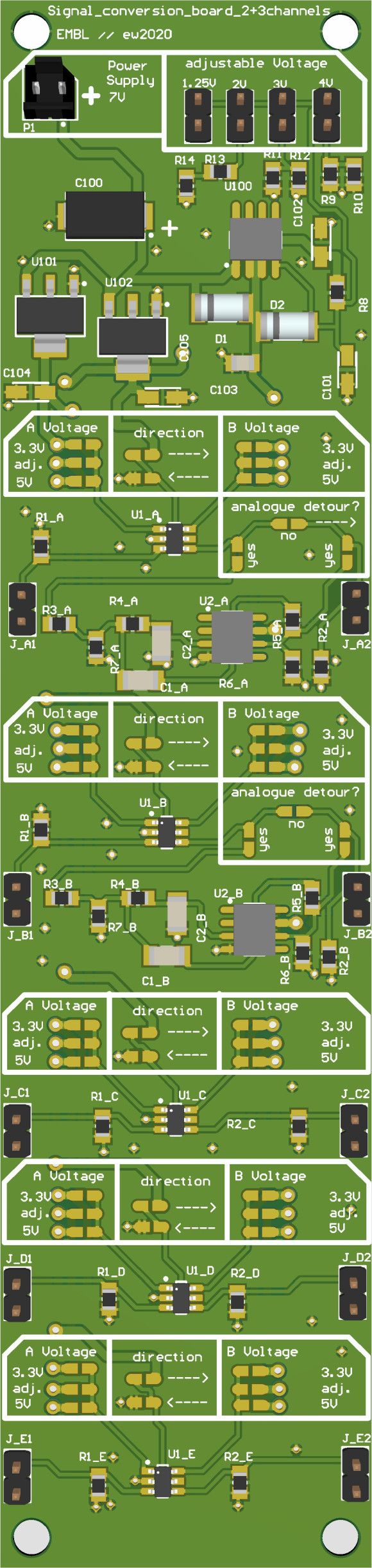
The signal conversion board is composed of 8 channels:
- 4 voltage conversion channels with optional low-pass filter.
- 4 bidirectional voltage conversion channels.
The channels only differ by the analog detour option. For the conversion channels without analog detour, or when the analog detour is ignored, the channels can be used in either direction: voltage A -> voltage B or B -> A. When the analog detour is soldered in, the voltage conversion is only performed A -> B. The low pass step is performed by a Sallen-Key circuit with a cut-off at 10 Hz.
In order to choose the input and output voltages, refer to the channel header:
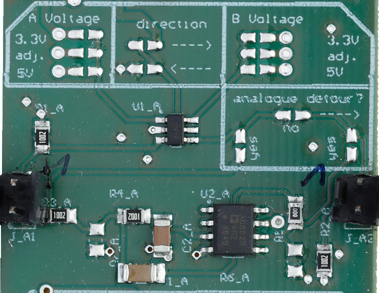
The channel header allows choosing the following parameters:
- Voltage A: 3.3 V, 4 V or 5 V. A single voltage must be chosen by soldering the two pads together.
- Direction: solder either "<---" or "--->" to choose the conversion direction between voltages A and B. If you are using the analog detour, choose "--->".
- Voltage B: 3.3 V, 4 V or 5 V. A single voltage must be chosen by soldering the two pads together.
- Analog detour: the analog detour is a low-pass RC filter that takes a PWM signal in input and output an analog signal. In order to use the analog detour, select the "A --> B" direction.
-
In order to supply a 3.3 V camera trigger to the FPGA, one channel from the signal conversion board can be used. First, select the direction by soldering the "--->" or "<---" path. Then, solder in the arrow's input the 5 V level, and in the arrow's output the 3.3 V level. If the channel contains an analog detour option, solder the "no" path.
-
Using a PWM channel from the FPGA as input A to one channel, we can create an analog output between 0-5 V by setting the A voltage to 3.3 V, the "--->" direction, voltage B as 5 V and soldering both "yes" pads on the analog detour. While the PWM signal is a digital signal with pulses between 1 and 2 ms, the output analog signal will have a voltage directly dependent on the PWM pulse length.
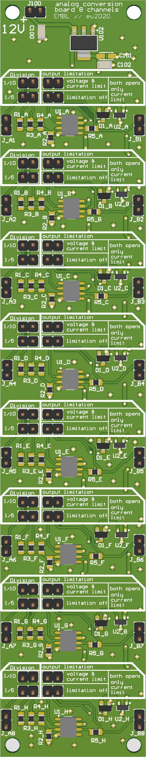
Since the Au FPGA analog input are limited to the 0-1 V range and are only safe up to 1.6 V, an additional circuit is necessary to convert commonly encountered 5 and 10 V inputs. The analog conversion board is composed of 8 channels allowing 1/10 or 1/5 voltage conversion. Additionally, the voltage and current limit can be disabled.
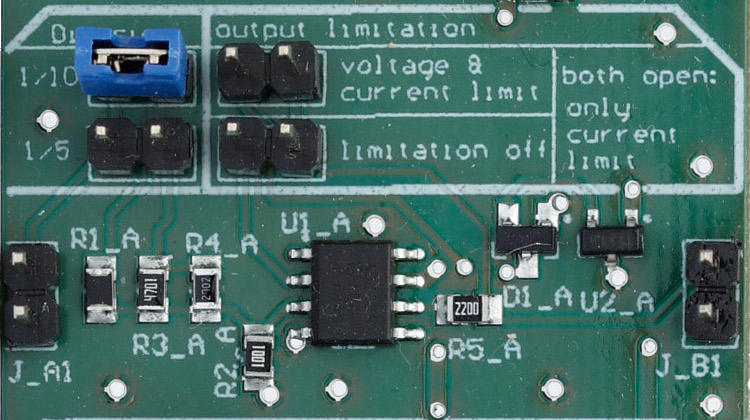
Each channel header present options that need to be jumped:
- Division: 1/10 or 1/5. One of the two division level must be chosen.
- Output limitation:
- Jumper on the voltage and current limit: the output voltage and current will be caped in order to prevent damages to the FPGA.
- Jumper on the limitation off: the output voltages and current will not be caped. This may endanger your FPGA.
- No jumper: only the output current is capped.
If a sensor on the microscope has an analog output comprised between 0 and 10 V, feeding it directly to the Au FPGA will saturate the read-out channel. Therefore, the signal is set as input of the conversion board, with the 1/10 option selected as well as the "voltage and current limitation" one. The output of the channel is then safe to be wired to the FPGA and the will allow reading out the signal.
Examples of applications are for instance monitoring the laser power meters or the focus of the microscope.
(soon)
(soon)
The AOTF-CB allows generating an analog output synchronized with the camera (in active or passive sync). It is best used with a PWM channel for the output level, and a laser trigger signal as synchronizing TTL input.
The main use case is setting laser power through an AOTF, thus allowing the laser to be synchronized with the camera, especially when direct TTL triggering is not available (e.g. DPSS lasers).
Alternatively, a faster PWM and a modified AOTF-CB (see tutorials), could allow fast synchronization compatible with galvo-mirrors for instance.